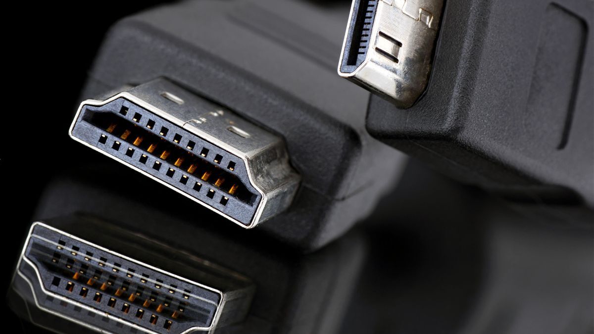
Based on this pin configuration, there’s only two dedicated power pins, which isn’t very good for large wattages. The rest are twinax signal pairs separated by ground to reduce crosstalk.
Usually when connectors are designed for power delivery, they’ll use bigger contacts to reduce the contact resistance (signal contacts tend to be small so you can fit more of them in the same space). I’m guessing the original DP connector form factor wasn’t made with such high power in mind, so it would make a lot of sense to use the spare signal pins for power delivery in this case. Running too much power through too few small pins can damage the contacts, by either by instant-welding the contact surfaces or by overheating the connector (see NVIDIA GPUs) ((also high voltages can cause arcing, which even in the best case will seriously degrade any connector)).
Take all of this with a huge grain of salt cause I just learned this stuff like a month ago, and my department has nothing to do with any of it. Just though someone might find it interesting.

It might? I think USB uses data lanes for power delivery above some point, and I wouldn’t be surprised if DP does the same.
Hi! I actually work at a major electrical connector company, so maybe I can shed some light on this.
I have no idea.
I used to work with electrical engineers, and whenever I asked about details, they’d shrug and say, “black magic?” Checks out.
Usually when connectors are designed for power delivery, they’ll use bigger contacts to reduce the contact resistance (signal contacts tend to be small so you can fit more of them in the same space). I’m guessing the original DP connector form factor wasn’t made with such high power in mind, so it would make a lot of sense to use the spare signal pins for power delivery in this case. Running too much power through too few small pins can damage the contacts, by either by instant-welding the contact surfaces or by overheating the connector (see NVIDIA GPUs) ((also high voltages can cause arcing, which even in the best case will seriously degrade any connector)).
Take all of this with a huge grain of salt cause I just learned this stuff like a month ago, and my department has nothing to do with any of it. Just though someone might find it interesting.