
Does this A in 18A stand for ångström? Can they even produce anything below 10 nm?
Yes, it does. It’s ambitious and a real stretch for Intel. But some are doubting this story of the yields being so low:
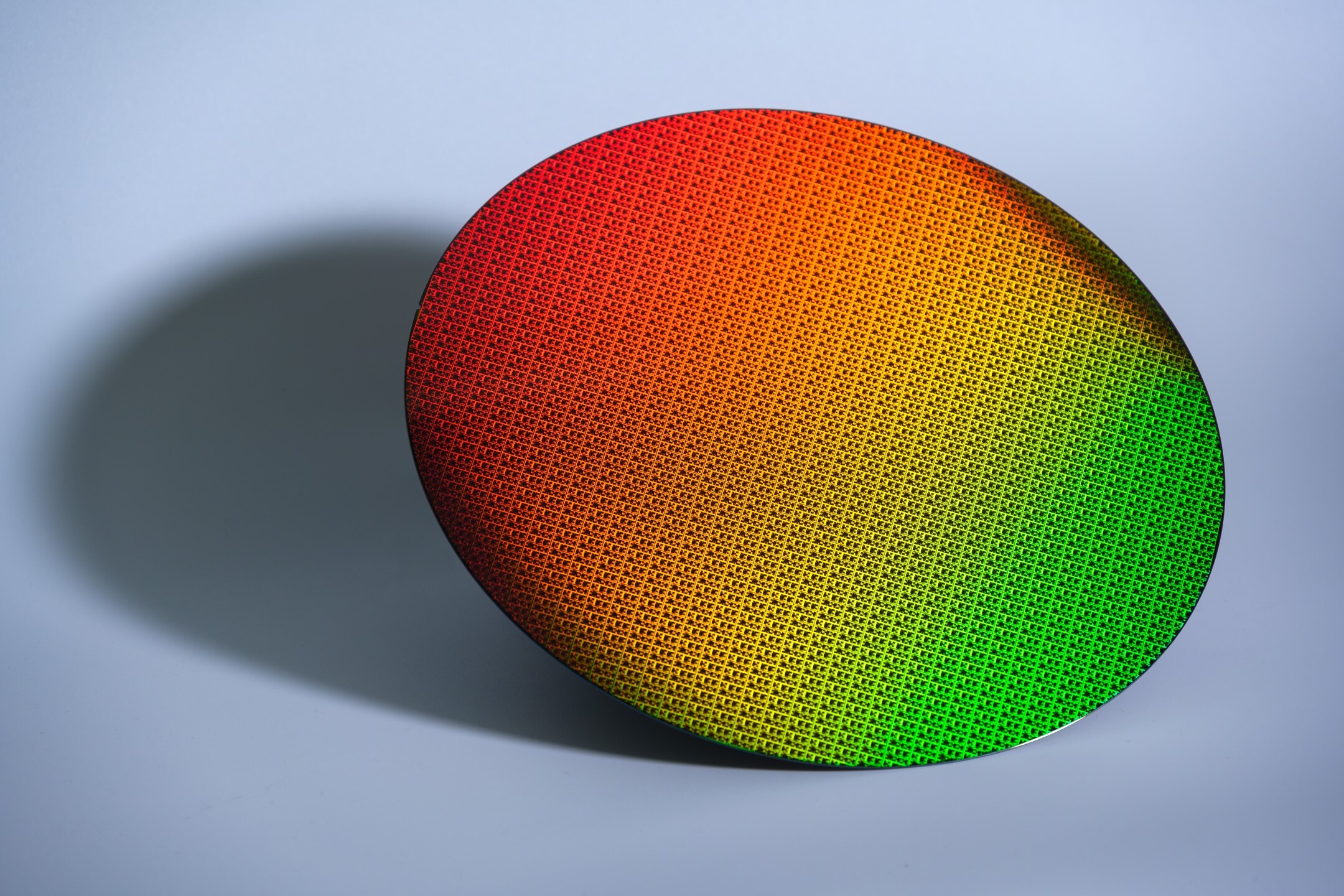
That wafer be lookin’ like a delicious mango in the thumbnail. 🤤
Maybe that’s why yields are so low? Employees keep eating them
I was curious how bad 10% was, so I went digging to see what it should be.
A “good” yield target on a modern process is something like 60-70%, so this is a shocking shockingly bad oof, though it’s also not a complete process, so it’s possible they can salvage this and turn it into something viable but, still, oof.
Talking about the “yield” of a process doesn’t make any sense. Yield is a metric for a specific chip fabricated on a given process. This depends heavily on the size of the chip and mitigation techniques.
The “correct” metric to compare processes is defect density (in defects per square cm). Intel claims that their defect density is below 0.4 defects/cm²: https://www.tomshardware.com/tech-industry/intel-says-defect-density-at-18a-is-healthy-potential-clients-are-lining-up. This would be relatively high but not much worse than what TSMC has seen for their recent nodes: https://www.techpowerup.com/forums/threads/intel-18a-process-node-clocks-an-abysmal-10-yield-report.329513/page-2#post-5387835).
Does this mean that errors happen on a later stage of production? How do we get from defects/cm to yield?
Yield is the percentage of chips that are functional. Roughly, you can think of it as the probability of a chip having 0 defects. The bigger the chip, or the higher the defect density, the lower this probability becomes. Chip designers will also include mitigation techniques (e.g. redundancy) to allow chips to work even with some defects.
For someone more in tune with the process, honest question: how is this not a failure on ASML, who makes the lithography machines? Or the company who makes the ultra pure silicon wafers? Is Intel just feeding unetchable garbage into the machines?
I have no idea about anything at all, but part of me wants to see this be the result of some predictable, stupid mistake, like a unit conversion error or something, and another part of me wants it to be something totally unpredictable, like some unique gravitational anomaly or some latent radiation of some kind, like, something with muons.
TSMC and Intel both use ASML lithography, but there are many many more steps than just lithography - Intel, TSMC, Samsung and other chipmakers use different processes to make the components on their chips (many of which are patented and so owned by specific parties).
These things include the physical structure of the components and wiring on the chip, how the silicon is doped and with what ions, what coatings are put on to be etched in the lithography and what coatings are applied to the etched layers, how the chips are packaged and also how multiple chips can be combined into one package.
Basically there are similarities but also hige differences between the different manufacturers, and a lot of trade secrets.
If you’re interested in this kind of thing, I’d recommend the youtube channel Asianometry - the content creator is amazing.
TSMC uses the same lithography and same wafers and gets working chips. It’s the fab process. Is it fixable? Idk.
I think there’s more to it - IIRC, this is Intel’s factory
Things that can mess up a batch- clean room not clean enough, vibrations from walking/vehicles/tectonic activity/lack of mechanical precision, temperature variations, impurities in chemicals or wafers, em interference, static charges, etc
We’re talking a few dozen atoms in the wrong place, the tolerances are minuscule when you’re making modern chips. A small problem in the supply chain, process, or the building itself could all kill your yield
I’m not an expert or anything, but I know this is a very unforgiving field
For the record, the TSMC N2 node being worked on experimentally at the moment (and is expected to be more performant than Intel’s 18A) currently has over 60% yields.
We don’t have exact figures on TSMC N4 (what AMD CPUs currently use), but reporting is widely that it is “over 80%”.
Wow, TSMC is absolutely killing it.
Never thought I’d see the absolute downfall of Intel in my lifetime but the last decade has not been good for them.
To be fair, they sat on their hands for a fair amount of it.